The NVIDIA H100 GPU contains 80 billion transistors. Each one is a microscopic switch made from silicon, smaller than a virus. They flip on and off trillions of times per second, performing the matrix math that powers the LLMs, image generators, and AI systems you use daily.
But how does a piece of silicon become a switch? How do you go from sand to a computer chip with 80 billion components?
The answer is semiconductors. Not just the chips themselves, but the physics that makes them possible. This is the bridge between the electricity basics from Post #1 and the processors we’ll cover in Post #3.
If you understand semiconductors, you understand why chip manufacturing is so hard. Why only a few companies can make advanced processors. And why the entire AI industry depends on what happens in a few buildings in Taiwan.
The Silicon Problem
Pure silicon is boring. At room temperature, it barely conducts electricity. It sits between conductors (like copper) and insulators (like rubber), which is why we call it a semiconductor.
Think of silicon like a dimmer switch. Regular conductors are light switches that are always on. Insulators are always off. Silicon is the dimmer you can adjust to control exactly how much current flows through.
But here’s the problem: pure silicon is stuck near the “off” position. To make it useful, you need to move the dimmer. That’s where doping comes in.
Silicon has four valence electrons. Each atom bonds with four neighbors in a crystal lattice, like a perfectly organized diamond structure.
Every electron locks in place, bonded to something. With no free electrons, almost no current flows.
Doping: Adding Impurities on Purpose
Doping solves the problem by contaminating silicon with specific impurities. Not random contamination. Precise, controlled addition of elements that have either three or five valence electrons instead of four.
The amount is tiny. One dopant atom per million silicon atoms. Sometimes one per billion. But that’s enough to change everything.
N-type: Extra Electrons
Add phosphorus (five valence electrons) to silicon. Four electrons bond with the silicon lattice. The fifth electron has nowhere to go, so it becomes free to move through the material.
Now you have charge carriers. Free electrons that can conduct current. This is N-type silicon (negative, because electrons are negative).
Think of it like adding salt to water. Pure water barely conducts electricity. Add a tiny bit of salt, and suddenly ions create a path for current. The salt doesn’t create current, it creates carriers that let current flow.
P-type: Missing Electrons
Add boron (three valence electrons) to silicon. All three electrons bond with the silicon lattice, but one bond lacks an electron. We call that missing electron a “hole.”
Holes aren’t real particles. They’re absences, like bubbles in water. But in semiconductor physics, they behave like positive charges. An electron from a neighboring atom can fill the hole, which effectively moves the hole to where the electron came from.
This is P-type silicon (positive, because holes act like positive charges).
The P-N Junction: Where It Gets Interesting
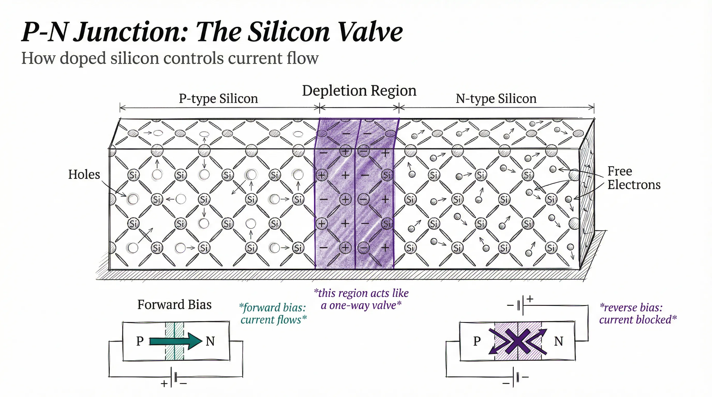
Now bring P-type and N-type silicon together. At their interface, something remarkable happens.
Free electrons from the N-side diffuse across the junction and fill holes on the P-side. Holes from the P-side diffuse the other direction and capture electrons. This creates a depletion region, a thin zone with no free charge carriers.
The depletion region acts like a valve. Apply voltage in one direction (forward bias) and current flows easily. Apply voltage in the other direction (reverse bias) and the depletion zone grows, blocking current.
This is a diode. A one-way valve for electricity. But diodes are just the warmup. The real breakthrough is transistors.
Transistors: The Three-Layer Trick
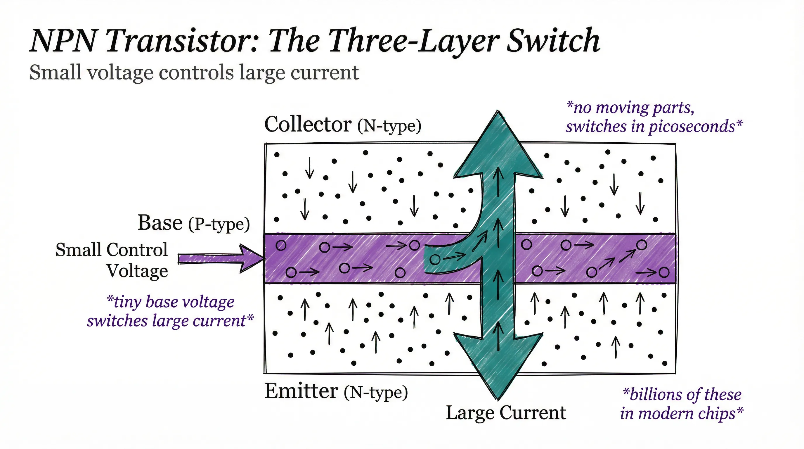
A transistor is three layers of semiconductor: NPN or PNP. Think of it as two P-N junctions back to back.
Think of a transistor like a water faucet. The faucet handle is the base. Turn the handle slightly (small input), and you control a large flow of water (large output current). The handle doesn’t need to move much water itself. It just controls the valve that lets the main flow through.
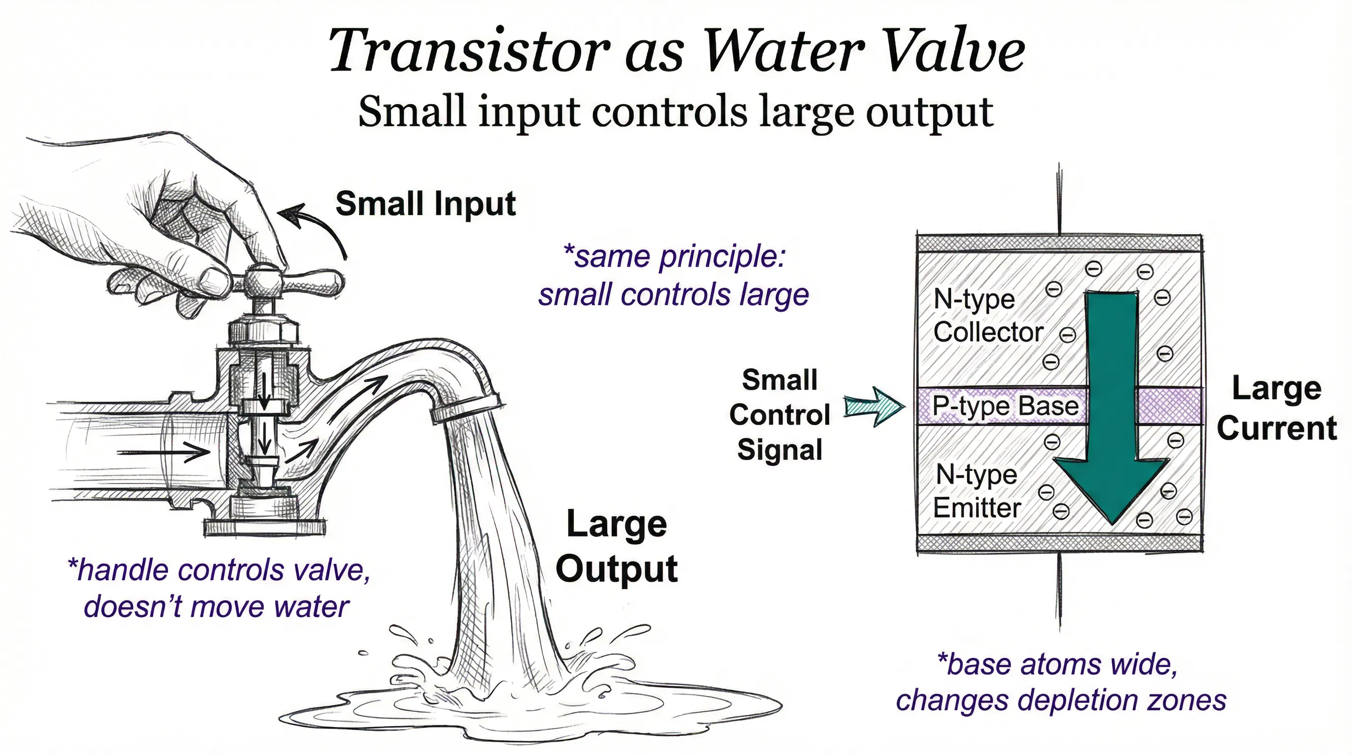
For an NPN transistor, you have N-type silicon (collector), then a thin P-type layer (base), then more N-type silicon (emitter). The magic happens at the base.
Apply a small voltage to the base and it controls a much larger current flowing from collector to emitter. A tiny signal switches or amplifies a big signal.
The base is deliberately thin, sometimes just a few atoms wide. When you apply voltage there, it changes the depletion zones in both P-N junctions simultaneously. This creates a path for electrons to flow from emitter to collector, even though there’s a P-type barrier in between.
This is why transistors changed everything:
- No moving parts: Unlike mechanical relays
- Fast switching: Modern transistors switch in picoseconds (trillionths of a second)
- Low power: Tiny amounts of energy to control large currents
- Scalable: Manufacturers can make them microscopically small
- Reliable: Billions of operations without mechanical failure
Bell Labs invented the first transistor in 1947. By 1971, Intel fit 2,300 of them onto a single chip (the 4004 processor).
Today, the NVIDIA B200 GPU has 208 billion transistors. That’s a 90 million times increase in 53 years.
From Transistors to Chips
Modern chips pack billions of transistors onto a piece of silicon smaller than your fingernail. We call this process photolithography.
Think of it like developing photographs, but instead of printing images on paper, you’re printing transistor patterns onto silicon using ultraviolet light.
The process:
- Coat a silicon wafer with light-sensitive material (photoresist)
- Shine UV light through a mask (pattern of transistors)
- Exposed areas become soluble
- Wash away exposed areas
- Etch or deposit materials in the pattern
- Remove remaining photoresist
- Repeat for the next layer
Modern chips have 50+ layers stacked on top of each other. Each layer adds more transistors, more connections, more complexity.
The Moore’s Law Progression
Here’s how transistor counts grew:
| Year | Chip | Transistor Count | Notes |
|---|---|---|---|
| 1971 | Intel 4004 | 2,300 | First microprocessor |
| 1989 | Intel 80486 | 1.2 million | Early PC era |
| 2000 | Pentium 4 | 42 million | Consumer desktop standard |
| 2010 | 6-core Intel | ~1 billion | Modern CPU era begins |
| 2022 | NVIDIA H100 | 80 billion | AI training workhorse |
| 2024 | NVIDIA B200 | 208 billion | Current record holder |
The node size (feature size of transistors) has shrunk from 10,000 nanometers (Intel 4004) to 3 nanometers (TSMC, 2024-2026). We’re approaching atomic scale limits.
Why smaller is better:
- Speed: Shorter distances mean faster signal travel
- Power efficiency: Less capacitance means less energy per switch
- Density: More transistors per chip means more compute
- Cost: More chips per wafer means lower cost per transistor
Why This Matters for AI
GPUs need billions of transistors because AI is parallel math at massive scale.
Training a neural network means multiplying matrices millions of times. Each multiplication involves thousands of parallel operations. More transistors means more parallel operations means faster training.
The NVIDIA H100 has 80 billion transistors organized into thousands of specialized cores. Each core can perform multiple operations simultaneously. That’s why GPUs dominate AI, not speed alone but parallel throughput.
The Power Catch
But there’s a catch: more transistors means more power consumption.
Remember from Post #1, every transistor switching consumes energy. The H100 draws 700W. The B200 draws 1,000W. Put 1,000 H100s in a data center and you need 700 kilowatts just for the GPUs, before cooling.
This is why electricity became the constraint we talked about in Post #1. More powerful AI needs more transistors. More transistors need more power. Power grids can’t expand fast enough.
The Semiconductor Bottleneck
Only a few companies can manufacture chips at the cutting edge:
- TSMC (Taiwan): 3nm process, makes chips for NVIDIA, Apple, AMD
- Samsung (South Korea): 3nm process, makes own chips and for others
- Intel (USA): Developing 3nm, mostly makes own designs
That’s it. Three companies control advanced chip manufacturing.
And there’s one more bottleneck: ASML (Netherlands) has a monopoly on extreme ultraviolet (EUV) lithography machines. These machines cost $150+ million each.
You need them to make chips below 7nm. Without ASML’s machines, you can’t make modern AI processors.
A single leading-edge fab costs $20+ billion to build. The equipment is so specialized that only one company makes it. The expertise required takes decades to develop.
This is why chip manufacturing is geopolitical. When TSMC’s Taiwan facilities face threats, the entire AI industry holds its breath.
Most advanced AI chips come from a 100-square-mile area that China considers part of its territory.
Understanding semiconductors means understanding that bottleneck.
The Physics Sets the Limits
AI progress isn’t just about better algorithms. Physics constrains it.
Moore’s Law (transistor count doubles every two years) held for 50 years, but it’s slowing. We’re approaching atomic scale limits.
At 3nm, transistor features span only about 15 silicon atoms. Go much smaller and quantum effects make transistors unreliable.
Power consumption scales with transistor count and switching speed. More compute means more heat. Data centers already spend as much on cooling as on electricity.
That won’t improve with denser chips. It gets worse.
The semiconductor supply chain is fragile. Design happens in the US. Manufacturing happens in Taiwan and South Korea. Materials come from Japan. Assembly happens in China.
One disruption anywhere breaks the chain.
The companies that understand these limits will make better decisions about which models to deploy, where to build infrastructure, and which hardware to buy.
What’s Next
Semiconductors bridge electricity and computation. They’re the material science that converts voltage into logic.
In Post #3, we’ll look at how transistors combine into processors. How CPUs and GPUs differ architecturally. Why GPUs dominate AI training. And why specialized chips (TPUs, NPUs) are emerging for specific workloads.
But the foundation is here: silicon, doping, P-N junctions, transistors, photolithography. Everything else builds on this.
References
-
Semiconductors and doping - Michigan State University - Educational resource on semiconductor physics fundamentals
-
p–n junction - Wikipedia - Detailed explanation of P-N junction physics and depletion region formation
-
Intel 4004 - Wikipedia - Historical context and specifications of the first microprocessor (2,300 transistors, 1971)
-
Transistor count - Wikipedia - Timeline of transistor count evolution from 4004 to modern 208B transistor chips
-
Moore’s law - Wikipedia - History of Moore’s Law and current challenges approaching atomic scale limits